Integrated Near Field sensOrs for high Resolution MicrowavE spectRoscopy (INFORMER)
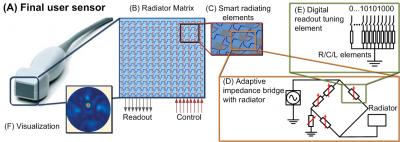
Informer will pursue the following research ideas: Resolution: In this project sub-wavelength radiators will be implemented with sub-micrometric precision using high-end IC technologies (i.e., CMOS 90nm), providing high resolution. Note that the resolution limitation in near-field imaging is not dictated by the operating frequency (in contrast to far-field systems such as radar), but by the feature size of the radiating elements. Inspection depth: To measure the electrical properties of tissues/biological samples below their immediate surface (e.g., up to a few millimeters of depth) we propose “dynamic” adjustment of the array elements and their properties using reconfigurable radiators structures implemented in high-end CMOS technology. Sensitivity: The evanescent wave radiators/detectors matrix will be combined with high-sensitivity detection circuitry placed on the same IC. The very-short distances between the antenna element and the detecting circuitry will allow compensation of the large impedance fluctuations of the radiators, due to the loading with different (bio-)samples, directly by the detection circuitry itself. The resulting wideband configuration facilitates free selection of the detection frequency such that the sample variations and anomalies can be detected with the highest sensitivity. With the proposed approach permittivity variations per pixel down to few percent will become detectable. Project focus is on the development of the novel “Smart near-field matrix sensors” operating up to 5GHz. New circuit and radiator concepts will be investigated for the design, implementation and calibration of the adjustable “pixel” radiator matrix sensor. The elements of this matrix will be directly connected to “selfmatching” high-precision, high-impedance detection bridges embedded by readout/control electronics. The implementation challenge of this novel sensor is addressed through the use of high-end silicon CMOS/BiCMOS technology, which offers the large-scale integration required for “pixel” detection circuitry, while simultaneously offering multiple, low-loss copper interconnect layers, needed for the realization of the array elements. This fully integrated approach provides significant advantages in size, reliability and cost, and as such will enable low-cost portable high resolution near-field sensors.

Project data
| Researchers: | Marco Spirito, Leo de Vreede, Michiel Pertijs, Gerasimos Vlachogiannakis, Harshitha Thippur Shivamurthy |
|---|---|
| Starting date: | March 2014 |
| Closing date: | March 2018 |
| Funding: | 492 kE; related to group 492 kE |
| Sponsor: | STW |
| Partners: | NXP, Keysight technologies BV |
| Contact: | Marco Spirito |